Virtual Tour
Lessons & Resources
Resources
- NCMN Facilities Video
- For Teachers: Nano/STEM Kits
- Cleanroom Virtual Tour:
Cleanroom Map
Click on the images below for more information.
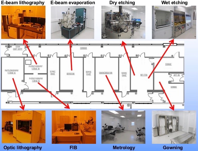
Learn about our Cleanroom
Entrance (Gowning)
A cleanroom or clean room is an environment, typically used in manufacturing, including of pharmaceutical products or scientific research, with a low level of environmental pollutants such as dust, airborne microbes, aerosol particles, and chemical vapors. More accurately, a cleanroom has a controlled level of contamination that is specified by the number of particles per cubic meter at a specified particle size. To give perspective, the ambient air outside in a typical urban environment contains 35,000,000 particles per cubic meter in the size range 0.5 μm and larger in diameter, corresponding to an ISO 9 cleanroom, while an ISO 1 cleanroom allows no particles in that size range and only 12 particles per cubic meter of 0.3 μm and smaller.
From Wikipedia under Creative Commons license.
Resources
More information at Support Center for Microsystems Education.
NNF's Cleanroom
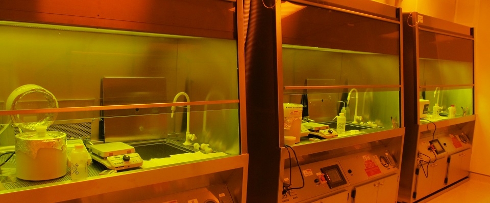
Etching Room (Dry and Wet Etching)
Etching is used in microfabrication to chemically remove layers from the surface of a wafer during manufacturing. Etching is a critically important process module, and every wafer undergoes many etching steps before it is complete.
For many etch steps, part of the wafer is protected from the etchant by a "masking" material which resists etching. In some cases, the masking material is a photoresist which has been patterned using photolithography.
The two fundamental types of etchants are liquid-phase ("wet") and plasma-phase ("dry"). Each of these exists in several varieties.
From Wikipedia under Creative Commons license.
Resources
- Etch Overview for Microsystems - Instructor Guide
- Etch Overview for Microsystems - Participant Guide
- Video: Microsystem Etch Process - Part 1
- Video: Microsystem Etch Process - Part 1
- Etch Overivew for Microsystems - PowerPoint
More information at Support Center for Microsystems Education.

By Mrneutrino (Own work) [GFDL or CC BY-SA 3.0], via Wikimedia Commons
Characterization (Metrology)
Characterization “Surface metrology” is the measurement of small-scale features on surfaces, and is a branch of metrology. Surface primary form, surface waviness and surface roughness are the parameters most commonly associated with the field. It is important to many disciplines and is mostly known for the machining of precision parts and assemblies which contain mating surfaces or which must operate with high internal pressures.
Surface finish may be measured in two ways: contact and non-contact methods. Contact methods involve dragging a measurement stylus across the surface; these instruments are called profilometers. Non-contact methods include: interferometry, confocal microscopy, focus variation, structured light, electrical capacitance, electron microscopy, and photogrammetry.
From Wikipedia under Creative Commons license.
Characterization at NNF
Deposition (E-beam Evaporation)
Resources
Nanoscale Electrodeposition Lesson
Science of Thin Films Lesson
YouTube Videos
- Deposition Overview - Part 1
- Deposition Overview - Part 2
- Wet Thermal Oxidation Process Animation
- Dry Thermal Oxidation Process Animation
- Wet vs. Dry Oxidation Process Animation
Other Resources
Deposition at NNF
More information at Support Center for Microsystems Education.
Photolithography (E-beam Lithography, Optic Lithography, FIB)
Photolithography, also termed optical lithography or UV lithography, is a process used in microfabrication to pattern parts of a thin film or the bulk of a substrate. It uses light to transfer a geometric pattern from a photomask to a light-sensitive chemical "photoresist", or simply "resist," on the substrate. A series of chemical treatments then either engraves the exposure pattern into, or enables deposition of a new material in the desired pattern upon, the material underneath the photo resist.
Photolithography shares some fundamental principles with photography in that the pattern in the etching resist is created by exposing it to light, either directly (without using a mask) or with a projected image using an optical mask. This procedure is comparable to a high precision version of the method used to make printed circuit boards. Subsequent stages in the process have more in common with etching than with lithographic printing. It is used because it can create extremely small patterns (down to a few tens of nanometers in size), it affords exact control over the shape and size of the objects it creates, and because it can create patterns over an entire surface cost-effectively.
Nanolithography is the branch of nanotechnology concerned with the study and application of fabricating nanometer-scale structures, meaning patterns with at least one lateral dimension between 1 and 100 nm. Different approaches can be categorized in serial or parallel, mask or maskless/direct-write, top-down or bottom-up, beam or tip-based, resist-based or resist-less methods. As of 2015, nanolithography is a very active area of research in academia and in industry. Applications of nanolithography include among others: Multigate devices such as Field effect transistors (FET), Quantum dots, Nanowires, Gratings, Zone plates and Photomasks, nanoelectromechanical systems (NEMS), or semiconductor integrated circuits (nanocircuitry).
From Wikipedia under Creative Commons license.
Resources
Photolithography Lesson
Hiding Behind the Mask Dry Etching Lesson
Nanoscale Electodeposition Lesson
PowerPoints
More information at Support Center for Microsystems Education.