Content
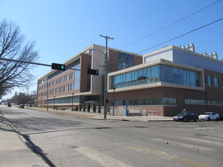
The vision of NNF is to be an internationally recognized center of excellence for nanoscience and an NNCI research hub for integrated fabrication, characterization, and education in nanotechnology for the Midwest. NNF includes eight central and shared facilities available to academic, industrial, and governmental users, with expert staff available for training, process consultation, and collaboration. Most NNF laboratories are located in the 32,000 sq. ft. Voelte-Keegan Nanoscience Research Center; others are in the attached Jorgensen Hall.
Facilities include state-of-the-art equipment for nanometer-scale characterization of materials surface and physical properties; hands-on access to electron microscopes, sample preparation equipment plus data collection and data reduction instrumentation; materials identification and characterization through x-ray diffraction techniques; three-dimensional characterization of nanostructures using electron beam imaging, chemical analysis, and diffraction; and a 4,000 square foot cleanroom for designing, fabricating, characterizing and testing of complex nano/micro-scale structures and devices.
The largest and strongest research areas of NNF users are nanomagnetics, nanoelectronics and sensors, and nanomaterials for energy. Essential research areas include synthesis, characterization & modeling of nanoscale materials/ structures, fundamental properties of electronic, magnetic, and structural materials at the nanoscale, emerging interface phenomena, and new functionalities not present in bulk materials. Research areas relevant to applications include nanomaterials for energy technologies, ultra-high-density data-storage media, nonvolatile memories and logic, nanoelectronics and spintronics, field and chemical sensors, and nanomanufacturing.